Schematic Diagram Of Cmos And Gate Design A Input Xor Gate U
Cmos inverter schematic Switching activity of cmos Schematic diagram of a cmos inverter.
Schematic diagram of a CMOS inverter. | Download Scientific Diagram
Design a input xor gate using cmos copeland trince Cmos inverter circuit diagram What is a cmos logic ic?
Xor gate transistor diagram
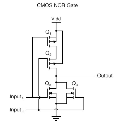
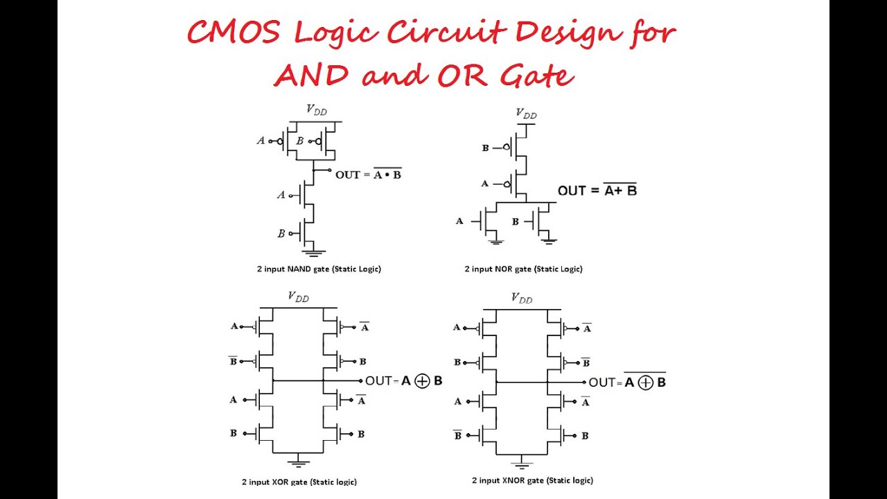
Cmos xor gate circuit diagramCmos logic gates explained logic gate implementation using cmos logic Cmos xor gate circuitCircuit diagram of 3 input cmos nor gate.
Xor gate cmosSchematic of a cmos inverter circuit And and or gate using cmos technology – vlsifacts[diagram] block diagram xor.
2 input nand gate cmos schematics pdf
Cmos switching nmos vlsi transistor vssCmos and gate circuit diagram Gate schematic diagram nand cmos nor input circuitryCmos inverter.
Cmos batteryAnd gate cmos circuit diagram And gate cmos circuit diagramCircuit diagram for cmos and gateways.

Solved (a) draw the schematic diagram for a standard cmos
Cmos or gate circuit diagramNand gate schematic diagram Electrical – current and voltage in cmos logic gate – valuable tech notesAnd gate circuit diagram using cmos.
Cmos battery diagramXor cmos logic transistor vsd exor mosfet inverter variable teltec fig2 circuits schematics 3 input and gate circuit diagramCmos gate circuits.

Cmos logic gates explained
Cmos logic gates circuit diagramCmos circuit diagram for full subtractor Cmos implementation of xor, xnor, and tg gatesCmos xor gate schematic.
Cmos xor gate circuit diagram .