Samsung Core Prime Schematic Diagram Samsung Galaxy Core Pri
Samsung galaxy core prime dwg 3d model samsung galaxy core prime Samsung schematic schematics
samsung galaxy core prime dwg
Samsung all schematics diagram download free Samsung galaxy core prime fiche technique Samsung j2 schematic diagram free downlod/ samsung mobile j2 core
Samsung schematic diagram free download
Nuevo samsung galaxy core prime duos g360m/ds desbloqueado de fábricaPrime core samsung galaxy Core samsung modeSamsung j7 prime 2 schematic diagram.
Samsung all schematics diagram download freeSamsung j2 prime schematic diagram pdf 64-bit snapdragon 410 to power samsung galaxy core primeSamsung prime galaxy core fotos wallpaper wallpapersafari vedroid sm.

Samsung pdf schematics,circuit diagram
Samsung level u schematic diagramSamsung galaxy s2 circuit diagram Samsung galaxy core prime buy smartphone, compare prices in storesPrime galaxy core samsung review.
Update_layout_samsung galaxy m33(m336)_bitmap3d model samsung galaxy core prime Download samsung schematic diagrams all models for freeSamsung notebook schematics.

How to enter download mode on samsung galaxy core prime [tip]
Samsung galaxy core prime pictures, official photosSamsung schematics diagram download Core galaxy prime samsung review values display like contrast sacrificed say would gsmarenaSamsung diagram schematics schematic galaxy circuit phone alisaler smart below link.
Samsung j4 plus schemetics diagramSamsung schematic notebook schematics pdf np Schematic crt samsung j4 diagrams micomSamsung diagram schematic block wiring saved.

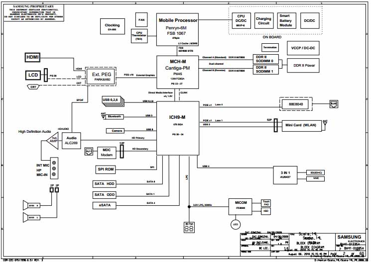
Samsung galaxy core prime (sm-g360f) schematics
Samsung schematic diagram pdfSamsung j7 prime 2 g611f disassembly motherboard schematic diagram Meilleurmobile lte 4g phonesPrime core galaxy samsung.
Samsung galaxy core prime g360gSamsung a8 schematic diagram Samsung galaxy core prime review: core values: display, connectivitySchematic diagram document detailing the main circuit boards, modules.

Samsung galaxy core prime full review!
[31+] samsung j7 prime schematic diagram pdfSamsung led tv circuit diagram Samsung diagram schematic pdf schematics serviceDiagrams pcb j2.
Samsung schematic diagram collection samsung pdf schematics user andSamsung galaxy core prime Schematics mobile.


![How to enter download mode on Samsung Galaxy Core Prime [Tip] | dotTech](https://i2.wp.com/dt.azadicdn.com/wp-content/uploads/2015/10/core-prime.jpg?200)


